Google reportedly developing ‘Frozen v2’ chip with Gemini’s architecture etched into the silicon — engineers project 6 to 10 times more tokens per watt than latest TPUs
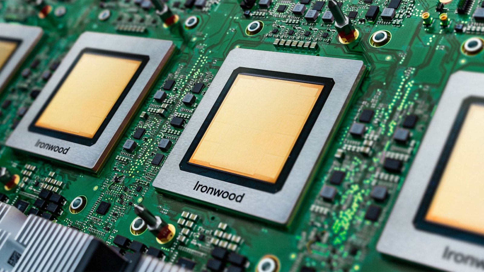
Google is developing a server chip, informally dubbed “Frozen v2,” that would etch part of its Gemini model’s architecture directly into the silicon, according to a report published Monday by The Information, citing two people with direct knowledge of the matter. Engineers on the project have projected that the chip could serve six to ten times more tokens per unit of power than the newest generation of Google’s TPUs, with deployment targeted for as soon as 2028. The two sources said the project is partly a response to an AI compute shortage severe enough that Google Cloud has turned down deals with outside customers.
Go deeper with TH Premium: AI and data centers
A TPU, like a GPU, runs whatever model is loaded onto it, which means the hardware makes time-consuming runtime decisions as it interacts with each one. Frozen v2 would have some of those decisions for Gemini fixed in the transistors, reducing the number of steps the chip takes and the amount of data it shuttles around per query. That could cut response latency enough to enable new applications, one of the sources said.
The original Frozen design, spearheaded by Google DeepMind chief scientist Jeff Dean, went further and would’ve baked Gemini’s weights themselves into the chip. Google set that proposal aside because silicon tied to a single model version would have too short a life cycle, according to the report. Frozen v2 freezes the architecture instead and leaves the weights updatable, so the chip stays useful across Gemini releases, but only for as long as Google builds them on the same underlying architecture. How much of the model to lock in is reportedly still undecided.

Google doesn’t plan to produce Frozen v2 at TPU volumes and views this generation partly as a trial run for more specialized silicon as model designs settle. The chip would sit alongside, rather than replace, a TPU line that split into separate training and inference variants with the eighth generation announced at Cloud Next in April. Its 2028 target also comes in the same year Google has reportedly booked Intel to package more than 3 million TPUs.
Model-hardwired inference silicon already exists in demonstrations. Taalas, a Toronto startup that has raised more than $200 million from investors including Quiet Capital and Fidelity, launched its HC1 chip in February with Llama 3.1 8B permanently wired into an 815mm-squared die built on TSMC’s N6 process. The company claims 17,000 tokens per second per user with no HBM on the package. Nvidia, meanwhile, struck a $20 billion deal in December to license technology from inference chip designer Groq.
Google hasn’t yet confirmed the project, with a spokesperson telling The Information that not every project moves into production and that “this rigorous exploration is central to our full stack approach.”

Follow Tom’s Hardware on Google News, or add us as a preferred source, to get our latest news, analysis, & reviews in your feeds.