Google’s Frozen v2 AI Chips to Redefine the AI Race
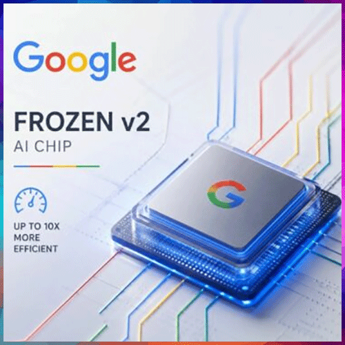
Every Gemini prompt activates Google’s custom AI chips inside its data centers, consuming compute power and energy to generate responses. With billions of queries processed daily, Google is developing Frozen v2, a next-generation AI chip projected to make Gemini 6–10 times more power-efficient per generated token, significantly reducing operating costs and improving AI scalability.
The artificial intelligence race is entering a new phase, with competition shifting from software innovation to custom silicon architecture. As AI models grow larger and more computationally intensive, technology giants are designing chips tailored specifically for their own AI systems to overcome rising energy costs, infrastructure constraints, and profitability challenges. The objective is no longer simply building the smartest AI model, but building the most efficient infrastructure to run it at scale.
How the Competition Compares
Google is far from alone in trying to wean itself off Nvidia and control its full hardware-software stack:
|
Company
|
Custom Chip
|
Primary Focus
|
Approach / Strategy
|
|
|
Frozen v2(2028)
|
Hyper-efficient Gemini Inference
|
Etches specific model architecture directly into the silicon for massive power savings.
|
|
OpenAI
|
Jalapeño(~2026)
|
LLM & Agentic Inference
|
A massive, blank-slate ASIC co-developed with Broadcom. Designed to support OpenAI models and potentially industry-wide LLMs close to theoretical hardware limits.
|
|
Microsoft
|
Maia
|
Cloud-wide AI Acceleration
|
Built to optimize a broad range of AI workloads across Azure, including Copilot and partner models.
|
|
Amazon
|
Trainium & Inferentia
|
Dual-Purpose AWS Infrastructure
|
A two-pronged strategy: Trainium handles massive model training, while Inferentia handles consumer-facing inference.
|
For years, the AI industry has depended heavily on NVIDIA’s general-purpose GPUs, which are powerful and flexible enough to support a wide range of AI workloads. However, their high cost, limited availability, and significant power consumption have encouraged companies to pursue Application-Specific Integrated Circuits (ASICs) optimized for their own AI architectures. These chips aim to maximize tokens per watt, reduce inference latency, and significantly lower operational costs.
Google is reportedly taking one of the industry’s most ambitious approaches through its next-generation AI chip, “Frozen v2.” Instead of designing a generic accelerator, the company is embedding elements of the Gemini model’s architecture directly into the silicon. By hardwiring portions of the model, Google expects to minimize unnecessary data movement and redundant computation, potentially delivering six to ten times greater efficiency than its current Tensor Processing Units (TPUs).
The strategy does involve trade-offs. Hardware optimized around a specific AI architecture can become obsolete if future models undergo major structural changes. To reduce that risk, Google plans to keep Gemini’s model weights updateable while maintaining compatibility with the underlying chip architecture, balancing efficiency with long-term usability.
Investor sentiment is also influencing this transition. As Alphabet’s AI infrastructure investments continue to climb toward $180–190 billion in capital expenditure, shareholders are demanding clear evidence of long-term returns. Reports outlining Google’s custom silicon roadmap helped reassure investors that the company has a credible plan to lower AI operating costs while improving energy efficiency, contributing to a positive market response.
The AI race is increasingly becoming a contest of infrastructure leadership rather than software capability alone. Companies that control their own chips, data centers, networking, storage, and AI software stack will gain significant advantages in cost, scalability, and performance. Google’s vertically integrated approach prioritizes maximum efficiency for Gemini, while competitors such as Microsoft and OpenAI appear to favor more flexible inference platforms capable of supporting diverse AI models and rapidly evolving workloads.
In the long run, the market is likely to support both strategies. Highly specialized silicon will dominate hyperscale AI deployments where efficiency and operating cost are critical, while flexible AI infrastructure will remain essential for enterprises serving multiple models and customer workloads. The future winners will be those that successfully balance performance, adaptability, energy efficiency, and return on investment, making custom silicon one of the defining battlegrounds in the next generation of artificial intelligence.